Applications

Avicena’s microLED interconnects are ideal for Scale Up applications, which require high shoreline density (> 1 Tbps/mm), ultra-low power (< 1 pJ/bit) connections with reaches up to 20 meters. This positions Avicena in the sweet spot between short reach copper (1 meter or less) and long reach optical interconnects (> 20 meters).

Copper dominates Scale Up today because it’s low cost, reliable and energy efficient. However, copper’s limited reach makes it impractical to scale beyond a few dozen GPUs. Standard optical technologies such as lasers and active optical cables are well suited to the longer connections between racks for Scale Out, but they’re too complex, power hungry and costly for Scale Up.

Unlike alternative approaches, Avicena’s µLED interconnects enable GPU clusters to Scale Up across multiple racks, linking thousands of GPUs, while achieving industry-leading sub-pJ/bit energy efficiency.

CPO
CPO remote HBMs LightBundle

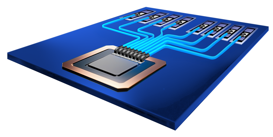
Optical Memory Interconnects address the unique challenge of moving data between processors and memory with low latency and high bandwidth. Like Scale Up, this requires high density bandwidth, ultra-low power, and short reach connections, as well as new techniques such as memory disaggregation. microLED interconnects are particularly well suited for memory disaggregation because the “wide & slow" architecture has 100s to 1,000s of lanes each running at data rates of a few Gbps. 

For example, one of the bottlenecks in processor to memory interactions is the physical layout and placement of memory chips around the microprocessor, which effectively limits total capacity. Memory disaggregation addresses this challenge by moving the High-Bandwidth Memory (HBM) away from the microprocessor, enabling larger memory banks. Avicena’s µLED interconnects with co-packaged optics provide high bandwidth connections between the microprocessor and memory banks.

Best-in-class energy efficiency and bandwidth density

While electrical interconnects work well over short distances of a few millimeters, they face fundamental limits in terms of reach, size and power efficiency, especially at higher data rates and longer distances. Avicena’s LightBundle™ interconnects use arrays of microLEDs connected via multi-core fiber bundles to Photo Detectors on CMOS ICs. This enables ultra-low power links of < 1 pJ/bit with over 10 meters reach.

LightBundle Interconnect Concept

Key Elements of LightBundle

Slow & wide reduces interconnect power

The parallel nature of the LightBundle interconnect is well matched to the wide internal bus architecture of ICs like CPUs, GPUs or switch ASICs, eliminating the need for a power intensive SerDes interface. In addition, Avicena’s LightBundle is a 2D µLED array making it possible for the IO to cover the entire IC area, thereby increasing the bandwidth density further.

Key Elements of LightBundle

Class leading bandwidth density

The figure illustrates how bandwidth density scales with per-lane data rates. With the current 4 Gbps lane data rate and 50 µm pitch, LightBundle™ achieves bandwidth densities > 2 Tbps/mm. The next generation of devices, featuring a reduced 25 µm pitch, will enable bandwidth densities exceeding 10 Tbps/mm.

Projected Shoreline Bandwidth Density vs Per-lane Data Rate

Beach Front Density & Energy Efficiency against Link Distance

5x better power and density

The performance of an interconnect can be expressed in terms of a figure of merit (FoM) combining bandwidth density on the edge of chip (Gbps/mm) with energy efficiency (pJ/bit). Avicena’s LightBundle™ optical interconnects can achieve power and density FoMs which are more than 5x better than existing solutions.

As shown in the chart, LightBundle interconnects match the performance of electrical links while increasing the reach to over 10 meters, allowing more efficient Scale Up AI architectures.

5x better power and density

The performance of an interconnect can be expressed in terms of a figure of merit (FoM) combining bandwidth density on the edge of chip (Gbps/mm) with energy efficiency (pJ/bit). Avicena’s LightBundle™ optical interconnects can achieve power and density FoMs which are more than 5x better than existing solutions.

Beach Front Density & Energy Efficiency against Link Distance