Best-in-class energy efficiency and bandwidth density
While electrical interconnects work well over short distances of a few millimeters, they face fundamental limits in terms of reach, size and power efficiency, especially at higher data rates and longer distances. Avicena’s LightBundle™ interconnects use arrays of microLEDs connected via multi-core fiber bundles to Photo Detectors on CMOS ICs. This enables ultra-low power links of < 1 pJ/bit with over 10 meters reach.
LightBundle Interconnect Concept
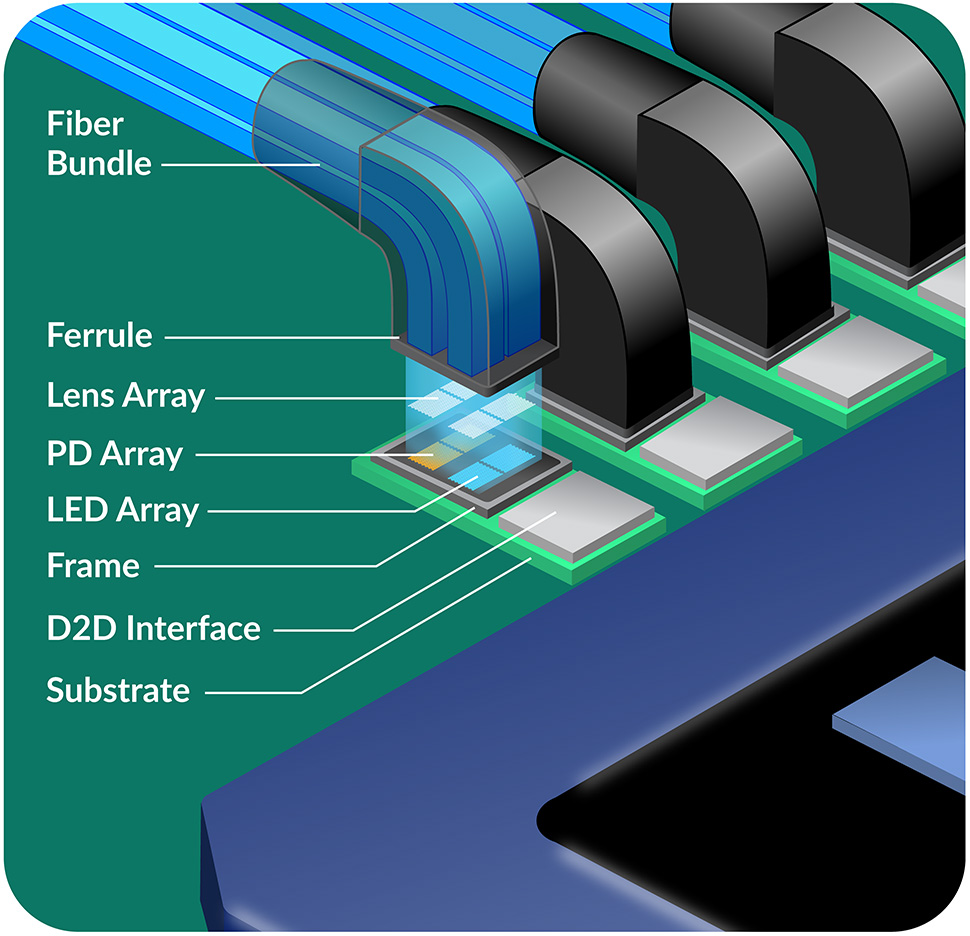
Key Elements of LightBundle
Slow & wide reduces interconnect power
The parallel nature of the LightBundle interconnect is well matched to the wide internal bus architecture of ICs like CPUs, GPUs or switch ASICs, eliminating the need for a power intensive SerDes interface. In addition, Avicena’s LightBundle is a 2D µLED array making it possible for the IO to cover the entire IC area, thereby increasing the bandwidth density further.
Key Elements of LightBundle
Class leading bandwidth density
The figure illustrates how bandwidth density scales with per-lane data rates. With the current 4 Gbps lane data rate and 50 µm pitch, LightBundle™ achieves bandwidth densities > 2 Tbps/mm. The next generation of devices, featuring a reduced 25 µm pitch, will enable bandwidth densities exceeding 10 Tbps/mm.
Projected Shoreline Bandwidth Density vs Per-lane Data Rate
Beach Front Density & Energy Efficiency against Link Distance
5x better power and density
The performance of an interconnect can be expressed in terms of a figure of merit (FoM) combining bandwidth density on the edge of chip (Gbps/mm) with energy efficiency (pJ/bit). Avicena’s LightBundle™ optical interconnects can achieve power and density FoMs which are more than 5x better than existing solutions.
As shown in the chart, LightBundle interconnects match the performance of electrical links while increasing the reach to over 10 meters, allowing more efficient Scale Up AI architectures.
5x better power and density
The performance of an interconnect can be expressed in terms of a figure of merit (FoM) combining bandwidth density on the edge of chip (Gbps/mm) with energy efficiency (pJ/bit). Avicena’s LightBundle™ optical interconnects can achieve power and density FoMs which are more than 5x better than existing solutions.
Beach Front Density & Energy Efficiency against Link Distance
See the light...
Avicena technology will be transformational in unlocking compute-to-memory chip-to-chip high-speed interconnects.